In preparation for the 2026 Canton Fair, mastering the art of Reverse Engineering Pcb is crucial. Dr. Emily Chen, an expert in electronic design, states, "Understanding existing products allows us to innovate and excel." As the fair presents opportunities in advanced manufacturing and electronics, leveraging this knowledge will be key.
The introduction of AI-enhanced search and smart navigation at the Canton Fair will reshape supplier selection. By filtering vendors based on certifications like ISO and CE, buyers gain a strategic edge. The efficiency of moving within a 1.55 million square meter venue becomes paramount.
Reverse Engineering PCB involves dissecting and analyzing existing designs. This practice not only aids in understanding competitors but also sparks innovation. Reflecting on previous projects, many find gaps in their knowledge. These gaps highlight the ongoing need for refinement and a better grasp of industry standards. As the Canton Fair approaches, ensuring a solid foundation in this area is essential for success.
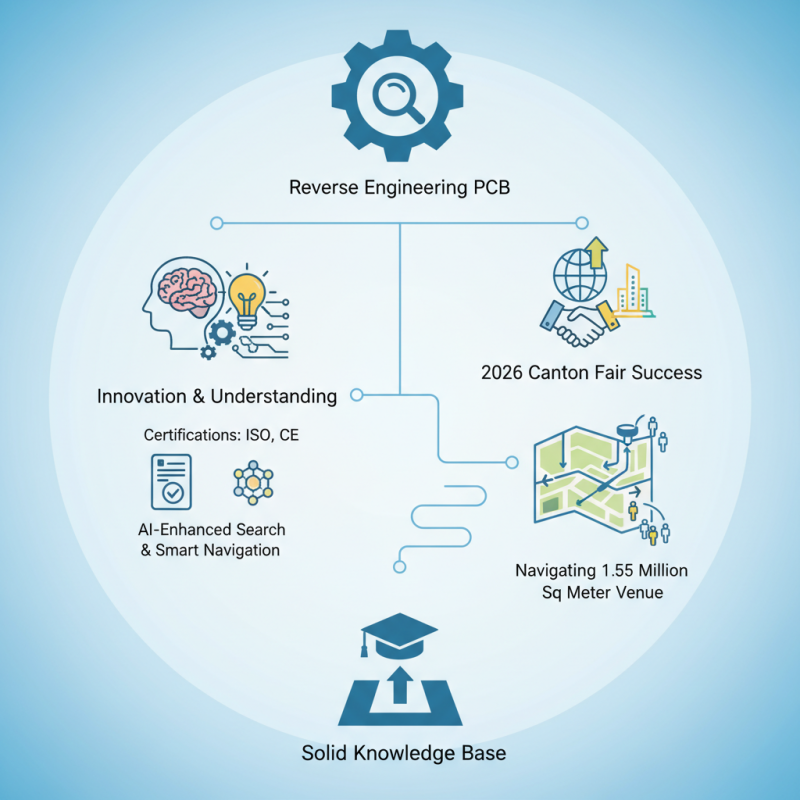
Reverse engineering printed circuit boards (PCBs) can be a valuable skill for those attending the 2026 Canton Fair. Understanding PCB design and engineering is crucial. Start with the basics of PCB structure. A typical PCB consists of layers, traces, and pads. The layout is essential for the functionality of electronic devices. Learning to recognize these components can help in identifying how they work together.
Focusing on PCB design tools is important. Software like CAD programs can aid in visualizing and creating designs. However, mastering these tools takes time and patience. Many individuals face challenges in grasping the interface. Mistakes often arise during the design process. These hiccups can be frustrating but serve as valuable learning experiences.
Additionally, it is vital to study existing PCBs. Analyze their layouts and connections. Look for common patterns and innovative designs. Each board tells a story about its intended function. Reflecting on what works and what doesn’t can enhance your understanding. Gaining insights from real-world examples can inspire better designs.
Reverse engineering a PCB can be a rewarding process. To succeed, one must identify key components and understand their functions. Each component on a PCB plays a vital role in the overall functionality of the device. Common components include resistors, capacitors, and integrated circuits. A resistor limits electrical flow. Its value is crucial for circuit performance.
Pay attention to the layout of these components. The placement can indicate their purpose. For instance, power supply lines often connect directly to ICs. This setup hints at their roles in power management. Take notes as you dissect each part of the board. You may find chips with unclear markings. This can lead to frustration. Sometimes, identifying these components requires additional research or tools.
When documenting your findings, draw diagrams. Visual aids can assist in understanding complex circuits. Afterward, reflect on potential areas for improvement. Were there components you overlooked? Did you misinterpret the function of a particular part? Analyzing these questions can enhance your learning and prepare you for future projects.
When preparing for the 2026 Canton Fair, understanding the tools and software for PCB reverse engineering is crucial. A recent industry report noted that over 75% of product developers rely on effective reverse engineering techniques. Tools such as PCB design software and analysis devices can significantly enhance understanding of PCB layouts and functions. These tools facilitate the examination of circuit board layers, components, and connections, allowing engineers to recreate designs efficiently.
Software like schematic capture tools is vital. They enable clear visualization of layouts. Data from a 2022 survey indicated that 62% of engineers found that utilizing such software reduced their project time by at least 30%. Agile methodologies have advanced, but many still struggle with adapting legacy boards. Failing to account for outdated designs can lead to inefficiencies and errors.
Moreover, various software packages offer simulation capabilities. These allow engineers to test circuit behaviors before physical production. With 56% of failures attributed to design flaws, integrating these tools is essential. Yet, many still neglect thorough testing and iteration. Reflecting on these lapses can lead to better practices and outcomes. The right blend of technology can illuminate the path to success at such an important venue.
Reverse engineering a PCB can seem daunting. However, with a structured approach, it becomes manageable. Start by carefully examining the board. Look for markings, connections, and components. Use a magnifying glass for small details. This will help you identify different parts. Take detailed notes during this process. Photographs can also capture intricate sections.
Next, create a schematic based on your observations. This step often requires patience. Don’t rush it. Struggling with the layout can lead to mistakes. Spend time ensuring all connections are accurate. A clear schematic will guide you in the next stages. If something feels unclear, revisit your notes. Oftentimes, small misconceptions can obscure the bigger picture.
Assemble a prototype once you are satisfied with the schematic. Test it thoroughly. Expect some unexpected behavior; it's part of the learning curve. If it doesn’t function as planned, analyze it with critical eyes. Adjustments may be necessary. Reflecting on errors can lead to a deeper understanding and future successes. Each attempt refines your skills for the upcoming Canton Fair. Embrace the process and learn from every challenge presented.
Reverse engineering printed circuit boards (PCBs) can provide a competitive edge at trade fairs, especially like the upcoming 2026 Canton Fair. A 2022 industry report indicated that companies leveraging reverse engineering saw a 30% boost in product innovation. By analyzing competitors' PCB designs, businesses can identify unique features and gaps in the market. This approach allows companies to refine their own products, creating better solutions that meet customer needs.
Many firms struggle with effective reverse engineering methods. A study revealed that approximately 40% of engineering teams felt unprepared to analyze complex designs. Having access to the right tools is crucial. Moreover, mapping out the PCB layers and components can be time-consuming and intricate. However, thorough documentation of findings can pay off. This includes noting potential improvements and the implications of utilizing such designs in new products.
There is risk involved too. Some reverse-engineered products may infringe on intellectual property rights, leading to legal issues. Balancing innovation and legality is tricky. Companies must tread carefully to ensure compliance, mitigating risks associated with aggressive copying tactics. Building a culture of ethical design while focusing on genuine innovation is essential for long-term success at trade events.
| Aspect | Description | Benefits |
|---|---|---|
| PCB Design Analysis | Understanding the layout and design components of existing PCBs. | Improved design efficiency and reduced development time. |
| Material Identification | Determining the materials used in competitor PCBs for better sourcing. | Cost-effective production and higher quality materials. |
| Functional Testing | Evaluating the performance of reverse engineered PCBs. | Ensuring reliability and performance standards. |
| Cost Analysis | Comparing production costs with competitors. | Identifying pricing strategies for better market positioning. |
| Market Trends | Studying recent market innovations and consumer preferences. | Aligning product development with market needs. |